Please read the instructions right through before starting work.
In order to keep the unit as simple as possible, and at the same time produce a usefully clean and symmetrical square wave which could have further applications, the discrete approach was abandoned.
The final square wave generator using an NE 555 IC has both a low component count and is simple to construct; it produces an excellent square wave, rich in harmonics (for signal tracing), and ample output to drive the capacitance bridge.
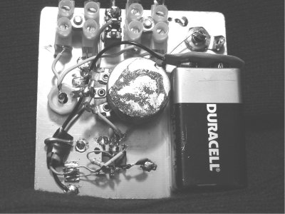
The whole unit in its basic form can be constructed on a piece of PCB only three inches square. If a capacitance substitution box - which in itself also has further application - is added, to extend the range and convenience of the bridge, the entire unit occupies 3" x 6". The unit is powered by a 9 volt PP3 battery.

The following instructions include the circuit, component list, comprehensive layout and connection diagrams, and photographs of the completed prototype (basic) unit.
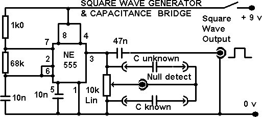
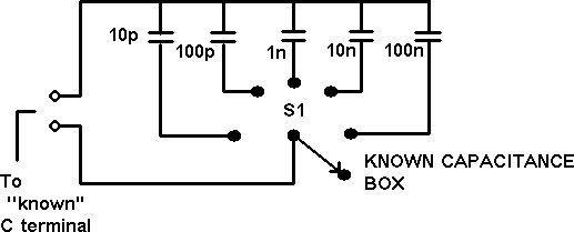
With the the values of resistors used, this circuit oscillates at about 1 kHz, producing a square wave of approximately equal mark / space ratio. Should it be necessary at a later date, the frequency may be altered between about 650 Hz and 7.2 kHz by altering the value of the 68k resistor between 10k and 160k. The range may be further extended by altering the value of the 10nF capacitor on pin 6 of the IC.
The mark / space ratio may be altered by changing the ratio of values of the two resistors, although the 1k resistor controls the circuit's current consumption, and should not be further reduced.
A near triangular wave form is available between pin 6 and earth rail.
The bridge circuit attached to pin 3 of the IC is a conventional Wheatstone Bridge arrangement. The Wheatstone Bridge basic circuit is shown in Fig. 3: with a signal source applied across the two arms of the bridge as shown, and either headphones or other null detector (such as the F&DARC audio amplifier / speaker project) connected across the bridge output, a null (minimum sound) will be heard when the ratio of the resistances is equivalent to the ratio of the capacitances, or R1 / R2 = C1 / C2.
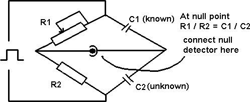
In the circuit of this project, R1 and R2 are replaced by a potentiometer; if C2 is a known value, the potentiometer control may be calibrated in terms of the ratio of the unknown to the known capacitors. Calibration instructions are included at the end of this article.
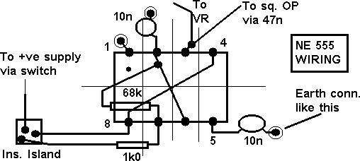
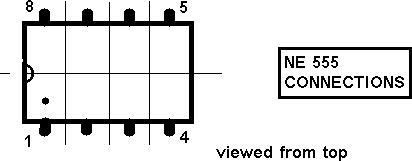
The square wave generator circuit wiring in the vicinity of the IC is shown in Fig. 5. This, and the photographs should help to clarify the recommended layout. A pin-out diagram for the NE 555 IC is given in Fig. 6. Note that this diagram shows the IC sitting on its pins, whereas the suggested layout uses the chip on its back (dead bug construction).
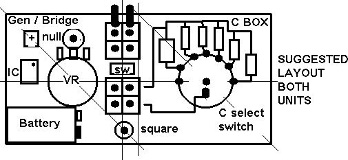
Complete the physical construction before wiring the IC: drill the bare board to accommodate the potentiometer, sockets, switches and choc blocks. Whilst the layout isn't critical, be sure to position the components so there's room to wire everything up, and especially so that there's room for the battery. In the layout diagrams, the light lines are construction lines, marking the board centre lines and diagonals which should help.
Note that the socket for the null indicator connection must be insulated from the board copper cladding. In the prototype a modified plastic bodied free (cable) socket was used. This was positioned so that the outer connection of the socket could be mechanically connected directly to the centre terminal of the potentiometer, which makes the assembly rigid.
Before starting to wire up the IC, make sure you're familiar with its connections and how pin 1 is marked. BE SURE TO PLACE THE IC ON THE BOARD SO THAT PIN 1 IS CLOSEST TO THE LEFT-HAND POTENTIOMETER TERMINAL.
The IC must be stuck down to the board with cyanoacrylate, or hot melt glue so that it forms a firm base for wiring up. All the other components are wired between its pins and either the earth plane or the insulated island (+ve battery connection), the potentiometer, or the choc block connector for the unknown capacitor. Note that the 47n capacitor is wired between that choc block and the centre pin of the square wave output socket.
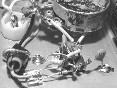
The insulated island is made from a 1/4" (6mm) square piece of PCB, stuck down on the base board with either cyanoacrylate or hot-melt glue.
One connector of each choc block is connected to the centre pin of the null indicator socket and has no other connections. The other connector of the "known" choc block is connected to the ground plane.
The battery connector is soldered between the on-off switch pole (+ve) and the ground plane. The switch "on" position is wired to the insulated island near the IC.
For the connection of the "unknown" capacitor to the unit (that's to the choc block nearest to the null indicator socket), and in the basic unit (as prototype) for the "known" capacitor also, modified crocodile clips are clamped into the choc block connectors. (4 required on basic unit).
The modification consists of soldering a piece of heavy gauge single wire to the inside of one arm only of each crocodile clip, so as to extend the arm by about half an inch (12mm). The crocodile clips are attached to the choc blocks by clamping their extended arms into the blocks.
Make sure that once clamped, the clip jaws are still free to move so that quick connections can be made.
If you're building the version with the capacitor substitution box added, you will only need two modified croc clips - for the "unknown" capacitor. You should also turn the "known" choc block anticlockwise by 90 degrees so that its connector protrudes from the long edge of the board.
Note that the photographs are of the prototype unit, in which the choc block connectors for "known" and "unknown" capacitors are transposed and do not accord with the suggested layout (Fig. 4) diagram.
If all is well, connect the 9v battery. Connect a pair of headphones or the F&DARC audio amplifier to the square wave output socket. If you use the amplifier, start with the volume turned down low!
Switch on, and a loud 1kHz rasping tone should be heard. If not, switch off and check your wiring again.
Once all is well, check additionally by connecting your headphone / amplifier to the null indicator socket. With neither "known" nor "unknown" in circuit, no tone should be heard.
Check that a tone is heard if either a "known" or an "unknown" capacitor is in circuit. If all is well you are ready to calibrate the unit.
This value is used since high precision e.g. silvered mica components are available in this value and in the range 1/10 to x10 of this capacitance (10pF to 1000pF). This factor range represents the maximum usable range of unknown which can be evaluated for any given value of "known" capacitor.
Connect a 10pF capacitor to the "unknown" terminal, and a null detector ('phones or amplifier) to the insulated phono connector. Switch on.
Adjust the potentiometer until you find the point on its travel where the sound is at a minimum, or disappears altogether (null point). This should be sharply defined, but it may be an advantage to increase the amplifier volume as an aid to precise detection of the exact null point. Volume should increase markedly to either side of the null point.
Mark the board at the pointer position with a datum mark and "0.1".
Repeat the exercise using a 1000pF capacitor as the "unknown". Mark the scale "10".
Further repeat the exercise with a 100pF "unknown". Mark the scale "1".
Now repeat the exercise using intermediate values of "unknown" over the range to fill in the gaps. Your calibration is now complete, and should hold good for other decade ranges also, i.e. "unknown" values between 1/10 and X10 of any value of "known" capacitor selected.
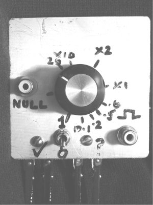
Arbitrarily select a "known" value and adjust the potentiometer for a null.
If the null appears to occur outside the range of the "known" value selected, select the next appropriate higher or lower "known" capacitor until the null is within range. Then read off the factor from the scale.
Multiply the factor by the value of the "known" capacitor to obtain the value of the "unknown"
Take the output from the Square Wave socket and apply to the circuit under test.
Note that if used with valve equipment, a series capacitor of at least 1000V rating MUST be connected in series with the output, and all appropriate precautions taken to avoid electric shock.
G7HEP 14/10/2002